MMCME2_ADV
时间: 2023-10-11 20:14:39 浏览: 69
MMCME2_ADV 是一种数字集成电路(Digital Integrated Circuit,简称DIC),它是一种可编程逻辑器件(Programmable Logic Device,简称PLD)的类型。MMCME2_ADV 是 Xilinx 公司生产的一款 PLD 的模块,用于实现时钟管理和时钟生成。
相关问题
[Place 30-575] Sub-optimal placement for a clock-capable IO pin and MMCM pair. If this sub optimal condition is acceptable for this design, you may use the CLOCK_DEDICATED_ROUTE constraint in the .xdc file to demote this message to a WARNING. However, the use of this override is highly discouraged. These examples can be used directly in the .xdc file to override this clock rule. < set_property CLOCK_DEDICATED_ROUTE BACKBONE [get_nets sys_clk_IBUF] > sys_clk_IBUF_inst (IBUF.O) is locked to IOB_X1Y74 instance_name/inst/mmcm_adv_inst (MMCME2_ADV.CLKIN1) is provisionally placed by clockplacer on MMCME2_ADV_X1Y2 The above error could possibly be related to other connected instances. Following is a list of all the related clock rules and their respective instances. Clock Rule: rule_mmcm_bufg Status: PASS Rule Description: An MMCM driving a BUFG must be placed on the same half side (top/bottom) of the device instance_name/inst/mmcm_adv_inst (MMCME2_ADV.CLKFBOUT) is provisionally placed by clockplacer on MMCME2_ADV_X1Y2 and instance_name/inst/clkf_buf (BUFG.I) is provisionally placed by clockplacer on BUFGCTRL_X0Y31
Based on the provided information, it seems that there is a sub-optimal placement for a clock-capable IO pin and MMCM pair in your design. If this condition is acceptable, you can use the CLOCK_DEDICATED_ROUTE constraint in the .xdc file to demote the message to a WARNING. However, using this override is highly discouraged.
To override this clock rule, you can add the following line in the .xdc file:
```
set_property CLOCK_DEDICATED_ROUTE BACKBONE [get_nets sys_clk_IBUF]
```
Please note that this error could possibly be related to other connected instances. The related clock rule "rule_mmcm_bufg" seems to be passing, but it's important to review all the clock rules and their respective instances to ensure proper placement.
If you have any further questions or need additional assistance, feel free to ask.
[DRC PDRC-34] MMCM_adv_ClkFrequency_div_no_dclk: The computed value 500.000 MHz (CLKIN1_PERIOD, net clk_in1_clk_wiz_main) for the VCO operating frequency of the MMCME2_ADV site MMCME2_ADV_X1Y5 (cell clk_wiz_main_inst/inst/mmcm_adv_inst) falls outside the operating range of the MMCM VCO frequency for this device (600.000 - 1440.000 MHz). The computed value is (CLKFBOUT_MULT_F * 1000 / (CLKINx_PERIOD * DIVCLK_DIVIDE)). Please run update_timing to update the MMCM settings. If that does not work, adjust either the input period CLKINx_PERIOD (10.000000), multiplication factor CLKFBOUT_MULT_F (5.000000) or the division factor DIVCLK_DIVIDE (1), in order to achieve a VCO frequency within the rated operating range for this device.如何解决
这个错误信息表明,您的设计中使用的时钟频率计算值超出了Xilinx器件的MMCM VCO频率的操作范围。具体来说,计算得到的VCO操作频率为500.000 MHz,而该器件的MMCM VCO频率的操作范围为600.000 - 1440.000 MHz。
要解决这个问题,有几种可能的方法:
1. 更新MMCM设置:按照错误信息中提到的建议,可以运行"update_timing"命令来更新MMCM设置。这个命令会根据当前的时钟约束和时序分析结果,自动调整MMCM的参数以确保VCO频率在操作范围内。
2. 调整输入周期:您可以尝试调整输入时钟的周期(CLKINx_PERIOD),使得计算得到的VCO频率在操作范围内。根据错误信息,当前的输入周期为10.000 ns。您可以根据需要适当增加或减小该值,然后重新运行时序分析和生成比特流文件。
3. 调整乘法因子和除法因子:另一个调整的选项是修改乘法因子(CLKFBOUT_MULT_F)和除法因子(DIVCLK_DIVIDE)。您可以根据实际需求适当增加或减小这两个因子的值,以使得计算得到的VCO频率在操作范围内。
需要注意的是,调整这些参数可能会对设计的时序和性能产生影响,因此在进行更改之前,建议您仔细评估和分析设计的需求和约束。另外,确保您的时钟源和外部电路也能够支持所需的时钟频率范围。
如果上述方法仍然无法解决问题,建议您参考Xilinx官方文档、用户指南和相关社区资源,以获取更详细的指导和支持。
相关推荐
最新推荐
ADV7511_Programming_Guide.pdf
ADV7511数据手册,软件编程人员使用。详细描述各个寄存器的配置方法。并包含ADV7511快速配置方案,方便软件工程师参考对ADV7511寄存器进行配置工作。
RTL8188FU-Linux-v5.7.4.2-36687.20200602.tar(20765).gz
REALTEK 8188FTV 8188eus 8188etv linux驱动程序稳定版本, 支持AP,STA 以及AP+STA 共存模式。 稳定支持linux4.0以上内核。
管理建模和仿真的文件
管理Boualem Benatallah引用此版本:布阿利姆·贝纳塔拉。管理建模和仿真。约瑟夫-傅立叶大学-格勒诺布尔第一大学,1996年。法语。NNT:电话:00345357HAL ID:电话:00345357https://theses.hal.science/tel-003453572008年12月9日提交HAL是一个多学科的开放存取档案馆,用于存放和传播科学研究论文,无论它们是否被公开。论文可以来自法国或国外的教学和研究机构,也可以来自公共或私人研究中心。L’archive ouverte pluridisciplinaire
:YOLO目标检测算法的挑战与机遇:数据质量、计算资源与算法优化,探索未来发展方向
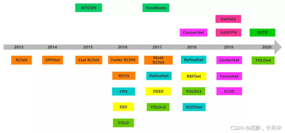
# 1. YOLO目标检测算法简介
YOLO(You Only Look Once)是一种
def ObjFun(x,y,beta): # 目标函数 """ Logistic regression loss function :param beta: model parameter vector :param x: feature matrix :param y: label vector :return: loss value """ n = x.shape[0] p = x.shape[1] pred = 1 / (1 + np.exp(-np.dot(x, beta))) pred = np.clip(pred, 1e-15, 1 - 1e-15) # 将预测值限制在一个很小的区间内 ObjVal = -np.sum(y * np.log(pred) + (1 - y) * np.log(1 - pred)) / n return ObjVal
好的,根据上面的目标函数,我们可以推导出其对应的梯度向量函数,如下所示:
def gradient(x, y, beta):
"""
Compute gradient of the logistic regression loss function
:param beta: model parameter vector
:param x: feature matrix
:param y: label vector
:return: gradient vector
"""
n = x.shape[0]
pred = 1 /
c++校园超市商品信息管理系统课程设计说明书(含源代码) (2).pdf
校园超市商品信息管理系统课程设计旨在帮助学生深入理解程序设计的基础知识,同时锻炼他们的实际操作能力。通过设计和实现一个校园超市商品信息管理系统,学生掌握了如何利用计算机科学与技术知识解决实际问题的能力。在课程设计过程中,学生需要对超市商品和销售员的关系进行有效管理,使系统功能更全面、实用,从而提高用户体验和便利性。
学生在课程设计过程中展现了积极的学习态度和纪律,没有缺勤情况,演示过程流畅且作品具有很强的使用价值。设计报告完整详细,展现了对问题的深入思考和解决能力。在答辩环节中,学生能够自信地回答问题,展示出扎实的专业知识和逻辑思维能力。教师对学生的表现予以肯定,认为学生在课程设计中表现出色,值得称赞。
整个课程设计过程包括平时成绩、报告成绩和演示与答辩成绩三个部分,其中平时表现占比20%,报告成绩占比40%,演示与答辩成绩占比40%。通过这三个部分的综合评定,最终为学生总成绩提供参考。总评分以百分制计算,全面评估学生在课程设计中的各项表现,最终为学生提供综合评价和反馈意见。
通过校园超市商品信息管理系统课程设计,学生不仅提升了对程序设计基础知识的理解与应用能力,同时也增强了团队协作和沟通能力。这一过程旨在培养学生综合运用技术解决问题的能力,为其未来的专业发展打下坚实基础。学生在进行校园超市商品信息管理系统课程设计过程中,不仅获得了理论知识的提升,同时也锻炼了实践能力和创新思维,为其未来的职业发展奠定了坚实基础。
校园超市商品信息管理系统课程设计的目的在于促进学生对程序设计基础知识的深入理解与掌握,同时培养学生解决实际问题的能力。通过对系统功能和用户需求的全面考量,学生设计了一个实用、高效的校园超市商品信息管理系统,为用户提供了更便捷、更高效的管理和使用体验。
综上所述,校园超市商品信息管理系统课程设计是一项旨在提升学生综合能力和实践技能的重要教学活动。通过此次设计,学生不仅深化了对程序设计基础知识的理解,还培养了解决实际问题的能力和团队合作精神。这一过程将为学生未来的专业发展提供坚实基础,使其在实际工作中能够胜任更多挑战。
"互动学习:行动中的多样性与论文攻读经历"
多样性她- 事实上SCI NCES你的时间表ECOLEDO C Tora SC和NCESPOUR l’Ingén学习互动,互动学习以行动为中心的强化学习学会互动,互动学习,以行动为中心的强化学习计算机科学博士论文于2021年9月28日在Villeneuve d'Asq公开支持马修·瑟林评审团主席法布里斯·勒菲弗尔阿维尼翁大学教授论文指导奥利维尔·皮耶昆谷歌研究教授:智囊团论文联合主任菲利普·普雷教授,大学。里尔/CRISTAL/因里亚报告员奥利维耶·西格德索邦大学报告员卢多维奇·德诺耶教授,Facebook /索邦大学审查员越南圣迈IMT Atlantic高级讲师邀请弗洛里安·斯特鲁布博士,Deepmind对于那些及时看到自己错误的人...3谢谢你首先,我要感谢我的两位博士生导师Olivier和Philippe。奥利维尔,"站在巨人的肩膀上"这句话对你来说完全有意义了。从科学上讲,你知道在这篇论文的(许多)错误中,你是我可以依
:YOLO目标检测算法的最佳实践:模型训练、超参数调优与部署优化,打造高性能目标检测系统

# 1. YOLO目标检测算法概述
**1.1 YOLO算法简介**
YOLO(You Only Look Once)是一种
pecl-memcache-php7 下载
你可以通过以下步骤来下载 pecl-memcache-php7:
1. 打开终端或命令行工具。
2. 输入以下命令:`git clone https://github.com/websupport-sk/pecl-memcache.git`
3. 进入下载的目录:`cd pecl-memcache`
4. 切换到 php7 分支:`git checkout php7`
5. 构建和安装扩展:`phpize && ./configure && make && sudo make install`
注意:在执行第5步之前,你需要确保已经安装了 PHP 和相应的开发工具。
建筑供配电系统相关课件.pptx
建筑供配电系统是建筑中的重要组成部分,负责为建筑内的设备和设施提供电力支持。在建筑供配电系统相关课件中介绍了建筑供配电系统的基本知识,其中提到了电路的基本概念。电路是电流流经的路径,由电源、负载、开关、保护装置和导线等组成。在电路中,涉及到电流、电压、电功率和电阻等基本物理量。电流是单位时间内电路中产生或消耗的电能,而电功率则是电流在单位时间内的功率。另外,电路的工作状态包括开路状态、短路状态和额定工作状态,各种电气设备都有其额定值,在满足这些额定条件下,电路处于正常工作状态。而交流电则是实际电力网中使用的电力形式,按照正弦规律变化,即使在需要直流电的行业也多是通过交流电整流获得。
建筑供配电系统的设计和运行是建筑工程中一个至关重要的环节,其正确性和稳定性直接关系到建筑物内部设备的正常运行和电力安全。通过了解建筑供配电系统的基本知识,可以更好地理解和应用这些原理,从而提高建筑电力系统的效率和可靠性。在课件中介绍了电工基本知识,包括电路的基本概念、电路的基本物理量和电路的工作状态。这些知识不仅对电气工程师和建筑设计师有用,也对一般人了解电力系统和用电有所帮助。
值得一提的是,建筑供配电系统在建筑工程中的重要性不仅仅是提供电力支持,更是为了确保建筑物的安全性。在建筑供配电系统设计中必须考虑到保护装置的设置,以确保电路在发生故障时及时切断电源,避免潜在危险。此外,在电气设备的选型和布置时也需要根据建筑的特点和需求进行合理规划,以提高电力系统的稳定性和安全性。
在实际应用中,建筑供配电系统的设计和建设需要考虑多个方面的因素,如建筑物的类型、规模、用途、电力需求、安全标准等。通过合理的设计和施工,可以确保建筑供配电系统的正常运行和安全性。同时,在建筑供配电系统的维护和管理方面也需要重视,定期检查和维护电气设备,及时发现和解决问题,以确保建筑物内部设备的正常使用。
总的来说,建筑供配电系统是建筑工程中不可或缺的一部分,其重要性不言而喻。通过学习建筑供配电系统的相关知识,可以更好地理解和应用这些原理,提高建筑电力系统的效率和可靠性,确保建筑物内部设备的正常运行和电力安全。建筑供配电系统的设计、建设、维护和管理都需要严谨细致,只有这样才能确保建筑物的电力系统稳定、安全、高效地运行。