
ACT2861QI
Rev 4.0, 17-Oct-2018
Innovative Power
TM
www.active-semi.com
ActiveSwitcher
TM
is a trademark of Active-Semi Copyright © 2018 Active-Semi, Inc.
18
FUNCTIONAL DESCRIPTION
General
ACT2861 is a buck-boost charger with integrated
MOSFETs. It provides a high efficiency, low external
component count, minimal size solution for 2 to 5 cell
battery charging applications. Its wide input operating
range of 4V to 29V allows charging from many input
sources.
The ACT2861 also operates in OTG (On-The-Go) mode
where it operates in reverse operation by converting the
battery voltage to a regulated output voltage on the VIN
pin. It autonomously switches between buck, buck-
boost, and boost modes depending on the input and
output voltages. It is optimized for minimum quiescent
current in shipping, shutdown, and standby modes. This
makes it ideal for battery powered applications. SHIP
mode reduces the total quiescent current to 1uA. It au-
tomatically resumes normal operation when the SHIPM
pin is pulled low or power is applied to VIN.
The ACT2861 can be operated in both stand-alone and
host-controlled applications. External resistors set the
fast charge current, input current limit, and OTG current
limit. Using host controlled I
2
C operation, the user has
full control over voltage, current, and fault settings. The
IC can be configured to charge any battery chemistry.
I
2
C operation gives the host full control of operating pa-
rameters as well as full knowledge of the operating pa-
rameters and fault conditions. A built in ADC provides
input voltage, output voltage, input current, output cur-
rent, and die temperature. The ADC also has one gen-
eral purpose input to measure an external analog signal.
The ACT2861 is highly flexible and contains many I
2
C
configurable functions. The IC’s default functionality is
defined by its default CMI (Code Matrix Index), but
much of this functionality can be changed via I
2
C. I
2
C
functionality includes OV and UV fault thresholds,
switching frequencies, current limits, precharge and fast
charge current settings, charging termination voltage,
JEITA settings, and more. The CMI Options section
shows the default settings for each available CMI option.
Contact sales@active-semi.com for additional infor-
mation about other configurations.
I
2
C Serial Interface
To ensure compatibility with a wide range of systems,
the ACT2861 uses standard I
2
C commands. It supports
clock speeds up to 1MHz. The ACT2861 always oper-
ates as a slave device, and can be factory configured to
one of two 7-bit slave addresses. The 7-bit slave ad-
dress is followed by an eighth bit, which indicates
whether the transaction is a read-operation or a write-
operation. Refer to each specific CMI for the IC’s slave
address
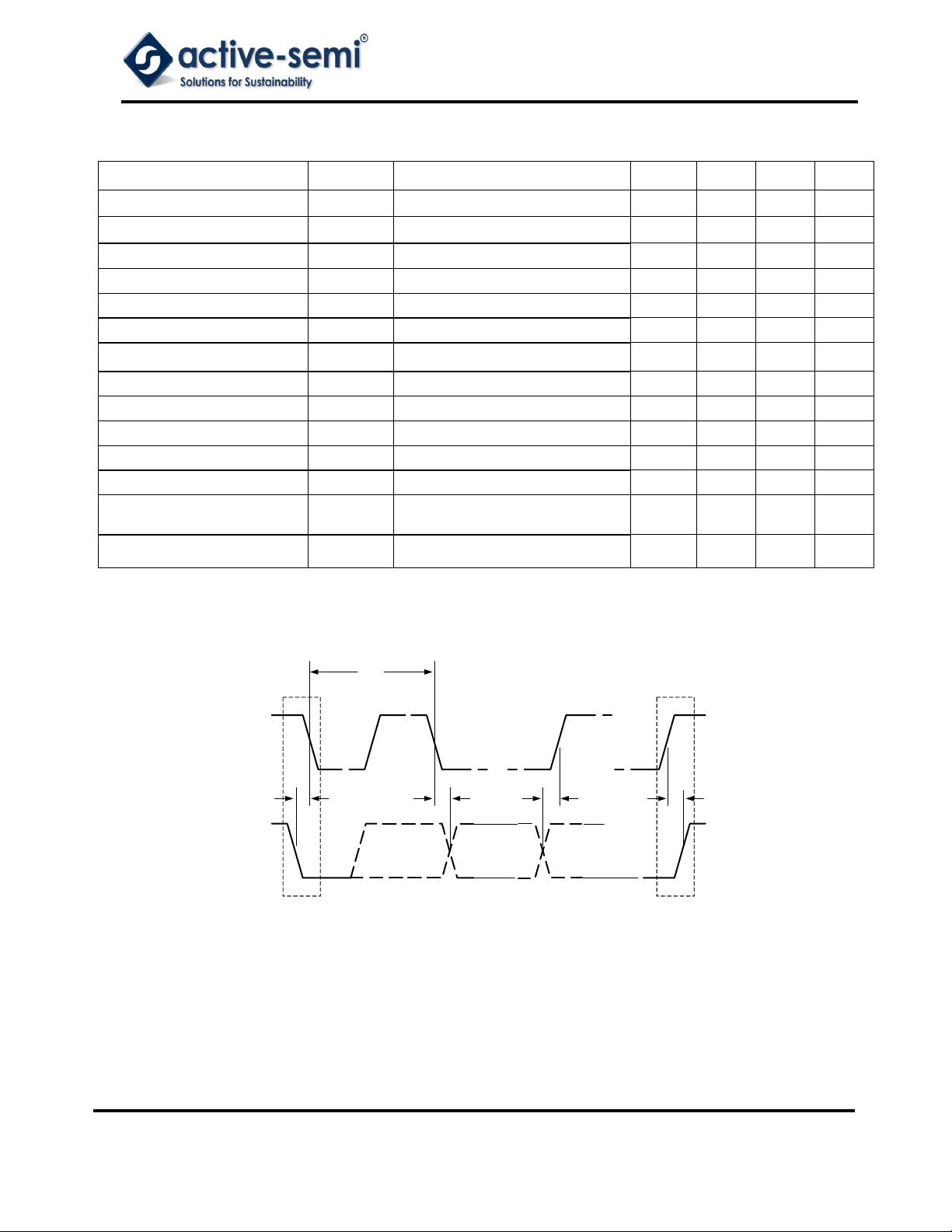
Table 1: ACT2861 I
2
C Addresses
7-Bit Slave Address 8-Bit Write
Address
8-Bit Read
Address
0x24h 010 0100b 0x48h 0x49h
0x66h 110 0110b 0xCCh 0xCDh
The I
2
C packet processing state machine has a 100ms
timeout function for each I
2
C command. If there is
greater than 100ms between a start bit and a stop bit,
the ACT2861 resets the I
2
C packet processing and sets
the I
2
C_FAULT bit in register 0x06h. Any time the I
2
C
state machine receives a start bit command, it immedi-
ately resets the packet processing, even if it is in the
middle of a valid packet. The I
2
C functionality is opera-
tional in all states except RESET.
I
2
C commands are communicated using the SCL and
SDA pins. SCL is the I
2
C serial clock input. SDA is the
data input and output. SDA is open drain and must have
a pull-up resistor. Signals on these pins must meet tim-
ing requirements in the Electrical Characteristics. For
more information regarding the I
2
C 2-wire serial inter-
face, refer to the NXP website: http://www.nxp.com.
I
2
C Registers
The ACT2861 has an array of internal registers that
contain the IC’s basic instructions for setting up the IC
configuration, output voltages, switching frequency,
fault thresholds, fault masks, etc. These registers give
the IC its operating flexibility. The two types of registers
are described below.
Basic Volatile – These are R/W (Read and Write) and
RO (Read only). After the IC is powered, the user can
modify the R/W register values to change IC functional-
ity. Changes in functionality include things like masking
certain faults. The RO registers communicate IC status
such as fault conditions. Any changes to these registers
are lost when power is recycled. The default values are
fixed and cannot be changed by the factory or the end
user.
Basic Non-Volatile – These are R/W and RO. After the
IC is powered, the user can modify the R/W register val-
ues to change IC functionality. Changes in functionality
include things like output voltage settings, startup delay
time, and current limit thresholds. Any changes to these
registers are lost when power is recycled. The default
values can be modified at the factory to optimize IC
functionality for specific applications. Please consult


 我的内容管理
展开
我的内容管理
展开


