
BTS6110-1SJA
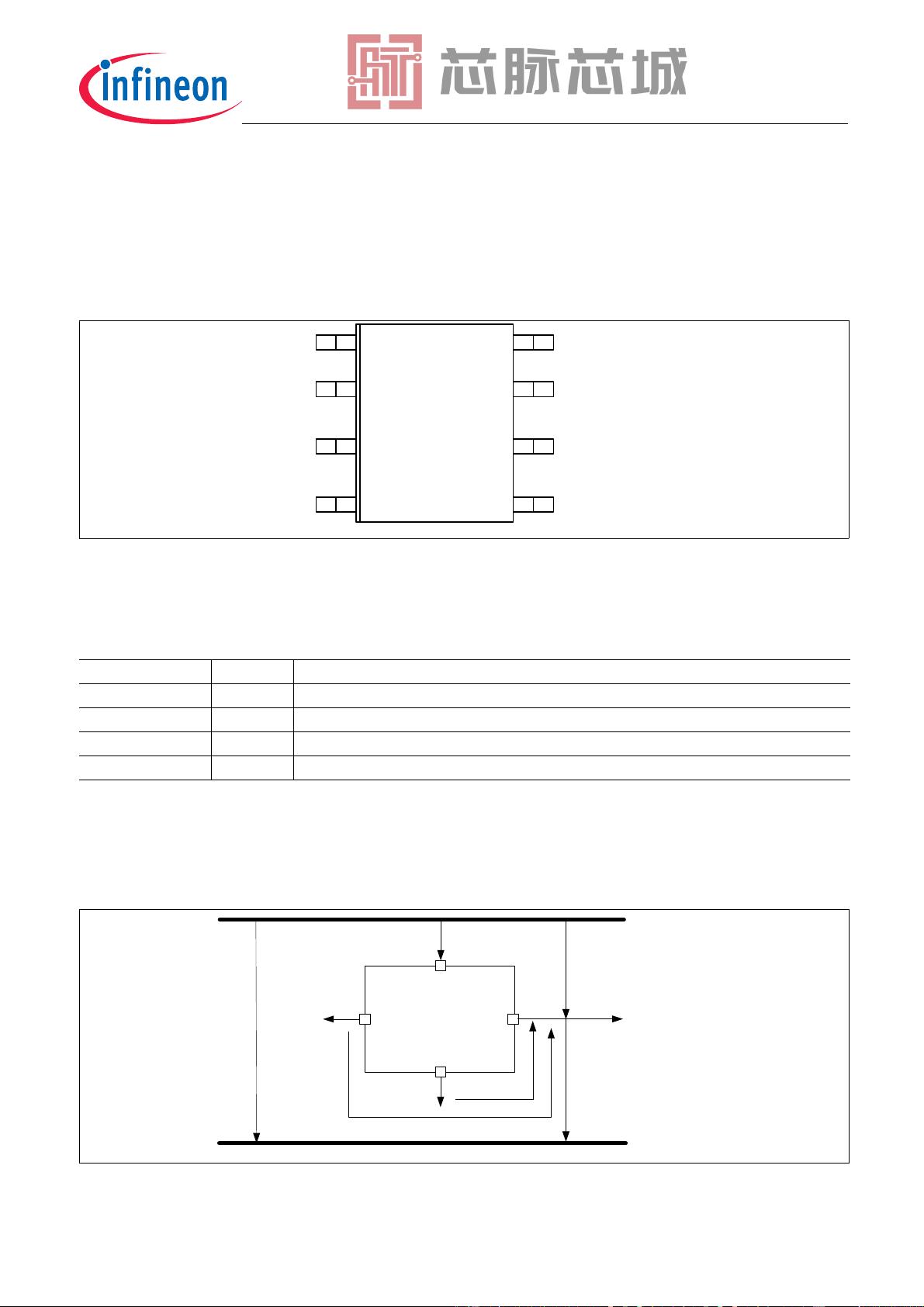
Pin Configuration
Data Sheet 5 Rev. 1.1, 2014-11-24
4 Pin Configuration
4.1 Pin Assignment
Figure 3 Pin Configuration
4.2 Pin Definitions and Functions
4.3 Voltage and Current Definition
Figure 4 shows all terms used in this document, with associated convention for positive values.
Figure 4 Voltage and Current Definition
Pin Symbol Function
1CAPCAPacitor; Must be connected to OUT via a reservoir capacitor
2 TEST TEST MODE PIN; Must be connected to OUT
3, 4 OUT OUTput; Protected high side power output channel
1)
1) All output pins must be connected together on the PCB. PCB traces have to be designed to withstand the maximum current
which can flow.
5, 6, 7, 8 V
S
Voltage Supply; Battery voltage
pinout Single SO 8. vsd
VS
VS
VS
CAP
TEST
OUT VS
1
3
2
8
7
6
45
OUT
V
S
CAP
OUT
V
S
V
CAP
I
S
V
DS
V
OUT
I
OUT
voltage and current convention single .vsd
+BAT
GND
I
CAP
TEST
V
TEST
I
TEST
剩余23页未读,继续阅读


