没有合适的资源?快使用搜索试试~ 我知道了~
首页美光DDR4 16GB芯片手册
资源详情
资源评论
资源推荐
TwinDie™ 1.2V DDR4 SDRAM
MT40A4G4 – 128 Meg x 4 x 16 Banks x 2 Ranks
MT40A2G8 – 64 Meg x 8 x 16 Banks x 2 Ranks
Description
The 16Gb (TwinDie™) DDR4 SDRAM uses
Micron’s 8Gb DDR4 SDRAM die (essentially two ranks
of the 8Gb DDR4 SDRAM). Refer to Micron’s 8Gb
DDR4 SDRAM data sheet for the specifications not in-
cluded in this document. Specifications for base part
number MT40A2G4 correlate to TwinDie manufactur-
ing part number MT40A4G4; specifications for base
part number MT40A1G8 correlate to TwinDie manu-
facturing part number MT40A2G8.
Features
• Uses 8Gb Micron die
• Two ranks (includes dual CS#, ODT, and CKE balls)
• Each rank has 4 groups of 4 internal banks for con-
current operation
• V
DD
= V
DDQ
= 1.2V (1.14–1.26V)
• 1.2V V
DDQ
-terminated I/O
• JEDEC-standard ball-out
• Low-profile package
• T
C
of 0°C to 95°C
– 0°C to 85°C: 8192 refresh cycles in 64ms
– 85°C to 95°C: 8192 refresh cycles in 32ms
Options Marking
• Configuration
– 128 Meg x 4 x 16 banks x 2 ranks 4G4
– 64 Meg x 8 x 16 banks x 2 ranks 2G8
• FBGA package (Pb-free)
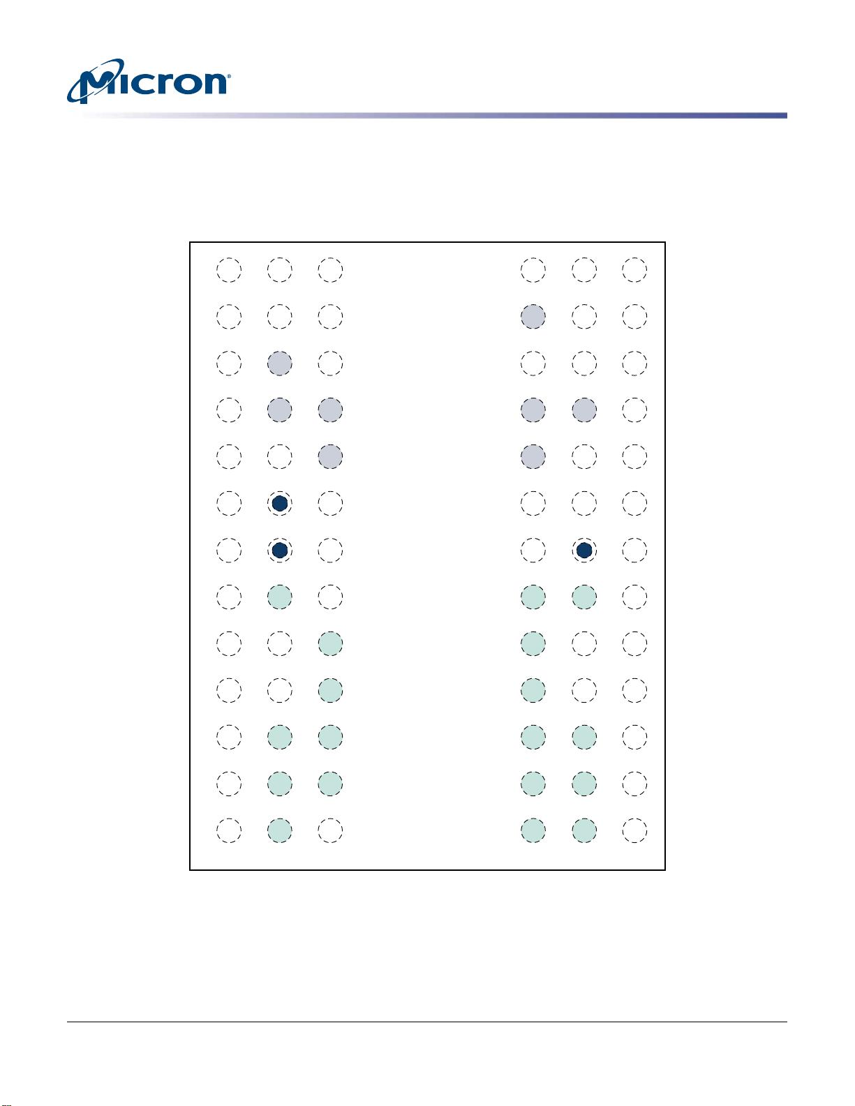
– 78-ball FBGA
(9.5mm x 13mm x 1.2mm) Die Rev :A
FSE
– 78-ball FBGA
(8.0mm x 12mm x 1.2mm) Die Rev :B
NRE
• Timing – cycle time
1
– 0.750ns @ CL = 18 (DDR4-2666) -075E
– 0.833ns @ CL = 16 (DDR4-2400) -083E
– 0.833ns @ CL = 17 (DDR4-2400) -083
– 0.937ns @ CL = 15 (DDR4-2133) -093E
– 0.937ns @ CL = 16 (DDR4-2133) -093
• Self refresh
– Standard None
• Operating temperature
– Commercial (0°C ≤ T
C
≤ 95°C) None
• Revision :A
:B
Note:
1. CL = CAS (READ) latency.
Table 1: Key Timing Parameters
Speed Grade
Data Rate
(MT/s) Target
t
RCD-
t
RP-CL
t
RCD (ns)
t
RP (ns) CL (ns)
-075E
1
2666 18-18-18 13.5 13.5 13.5
-083E
2
2400 16-16-16 13.32 13.32 13.32
-083
2
2400 17-17-17 14.16 14.16 14.16
-093E 2133 15-15-15 14.06 14.06 14.06
-093 2133 16-16-16 15 15 15
Notes:
1. Backward compatible to 1600, CL = 11; 1866, CL = 13; 2133, CL = 15; and 2400, CL = 17.
2. Backward compatible to 2133, CL = 15 (-093E).
16Gb: x4, x8 TwinDie DDR4 SDRAM
Description
PDF: 09005aef85fd40a1
DDR4_16Gb_x4_x8_2CS_TwinDie.pdf - Rev. D 12/16 EN
1
Micron Technology, Inc. reserves the right to change products or specifications without notice.
© 2015 Micron Technology, Inc. All rights reserved.
Products and specifications discussed herein are subject to change by Micron without notice.
Table 2: Addressing
Parameter 4096 Meg x 4 2048 Meg x 8
Configuration 128 Meg x 4 x 16 banks x 2 ranks 64 Meg x 8 x 16 banks x 2 ranks
Bank group address BG[1:0] BG[1:0]
Bank count per group 4 4
Bank address in bank group BA[1:0] BA[1:0]
Row address 128K A[16:0] 64K A[15:0]
Column address 1K A[9:0] 1K A[9:0]
16Gb: x4, x8 TwinDie DDR4 SDRAM
Description
PDF: 09005aef85fd40a1
DDR4_16Gb_x4_x8_2CS_TwinDie.pdf - Rev. D 12/16 EN
2
Micron Technology, Inc. reserves the right to change products or specifications without notice.
© 2015 Micron Technology, Inc. All rights reserved.
Ball Assignments and Descriptions
Figure 1: 78-Ball FBGA Ball Assignments (Top View)
1 2 3 4 6 7 8 95
V
DD
V
PP
V
DDQ
V
SSQ
V
SS
V
DD
V
SS
V
DD
V
REFCA
V
SS
RESET_n
V
DD
V
SS
V
SSQ
V
DDQ
DQ0
DQ4/NC
V
DDQ
C2/ODT1
C0/CKE1
WE_n/A14
BG0
BA0
A6
A8
A11
V
SSQ
V
DDQ
V
SS
DQ5/NC
V
DDQ
CK_c
C1/CS1_n
RAS_n/A16
BG1
BA1
A5
A7
A13
V
SSQ
ZQ
V
DDQ
V
SSQ
V
SS
V
DD
RFU/TEN
V
SS
V
DD
V
SS
ALERT_n
V
PP
V
DD
A
B
C
D
E
F
G
H
J
K
L
M
N
A
B
C
D
E
F
G
H
J
K
L
M
N
NF, NF/DM_n/
DBI_n/TDQS_t
DQ1
V
DD
DQ3
DQ7/NC
CK_t
CS_n
CAS_n/A15
A12/BC_n
A3
A1
A9
A17/NC
NF, NF/
TDQS_c
DQS_c
DQS_t
DQ2
DQ6/NC
ODT
CKE
ACT_n
A10/AP
A4
A0
A2
PAR
Notes:
1. See the FBGA 78-Ball Descriptions table.
2. Dark balls (with ring) designate balls that are specific to controlling the second die of
the TwinDie package when compared to a monolithic package.
3. A comma “,” separates the configuration; a slash “/” defines a selectable function. For
example: Ball A7 = NF, NF/DM_n/DBI_n/TDQS_t where NF applies to the x4 configuration
only. NF/DM_n/DBI_n/TDQS_t applies to the x8 configuration only and is selectable be-
tween NF, DM_n, DBI_n, or TDQS_t via MRS.
16Gb: x4, x8 TwinDie DDR4 SDRAM
Ball Assignments and Descriptions
PDF: 09005aef85fd40a1
DDR4_16Gb_x4_x8_2CS_TwinDie.pdf - Rev. D 12/16 EN
3
Micron Technology, Inc. reserves the right to change products or specifications without notice.
© 2015 Micron Technology, Inc. All rights reserved.
Table 3: FBGA 78-Ball Descriptions
Symbol Type Description
A[17:0] Input Address inputs: Provide the row address for ACTIVATE commands and the col-
umn address for READ/WRITE commands to select one location out of the memo-
ry array in the respective bank. (A10/AP, A12/BC_n, WE_n/A14, CAS_n/A15, RAS_n/
A16, have additional functions; see individual entries in this table). The address
inputs also provide the op-code during the MODE REGISTER SET command. A16 is
used on some 8Gb and 16Gb parts, and A17 is only used on some 16Gb parts.
A10/AP Input Auto precharge: A10 is sampled during READ and WRITE commands to deter-
mine whether auto precharge should be performed to the accessed bank after a
READ or WRITE operation (HIGH = auto precharge; LOW = no auto precharge).
A10 is sampled during a PRECHARGE command to determine whether the PRE-
CHARGE applies to one bank (A10 LOW) or all banks (A10 HIGH). If only one
bank is to be precharged, the bank is selected by the bank group and bank ad-
dresses.
A12/BC_n Input Burst chop: A12/BC_n is sampled during READ and WRITE commands to deter-
mine if burst chop (on-the-fly) will be performed. (HIGH = no burst chop; LOW =
burst-chopped). See the Command Truth Table.
ACT_n Input Command input: ACT_n indicates an ACTIVATE command. When ACT_n (along
with CS_n) is LOW, the input pins RAS_n/A16, CAS_n/A15, and WE_n/A14 are trea-
ted as row address inputs for the ACTIVATE command. When ACT_n is HIGH
(along with CS_n LOW), the input pins RAS_n/ A16, CAS_n/A15, and WE_n/A14
are treated as normal commands that use the RAS_n, CAS_n, and WE_n signals.
See the Command Truth Table.
BA[1:0] Input Bank address inputs: Define the bank (within a bank group) to which an ACTI-
VATE, READ, WRITE, or PRECHARGE command is being applied. Also determines
which mode register is to be accessed during a MODE REGISTER SET command.
BG[1:0] Input Bank group address inputs: Define the bank group to which a REFRESH, ACTI-
VATE, READ, WRITE, or PRECHARGE command is being applied. Also determines
which mode register is to be accessed during a MODE REGISTER SET command.
BG[1:0] are used in the x4 and x8 configurations.
C0/CKE1,
C1/CS1_n,
C2/ODT1
Input Stack address inputs: These inputs are used only when devices are stacked;
that is, 2H, 4H, and 8H stacks for x4 and x8 configurations (these pins are not
used in the x16 configuration). DDR4 will support a traditional dual-die package
(DDP), which uses these three signals for control of the second die (CS1_n, CKE1,
ODT1). DDR4 is not expected to support a traditional quad-die package (QDP).
For all other stack configurations, such as a 4H or 8H, it is assumed to be a single-
load (master/slave) type of configuration where C0, C1, and C2 are used as chip
ID selects in conjunction with a single CS_n, CKE, and ODT.
CK_t,
CK_c
Input Clock: Differential clock inputs. All address, command, and control input signals
are sampled on the crossing of the positive edge of CK_t and the negative edge
of CK_c.
16Gb: x4, x8 TwinDie DDR4 SDRAM
Ball Assignments and Descriptions
PDF: 09005aef85fd40a1
DDR4_16Gb_x4_x8_2CS_TwinDie.pdf - Rev. D 12/16 EN
4
Micron Technology, Inc. reserves the right to change products or specifications without notice.
© 2015 Micron Technology, Inc. All rights reserved.
Table 3: FBGA 78-Ball Descriptions (Continued)
Symbol Type Description
CKE Input Clock enable: CKE HIGH activates, and CKE LOW deactivates, the internal clock
signals, device input buffers, and output drivers. Taking CKE LOW provides PRE-
CHARGE POWER-DOWN and SELF REFRESH operations (all banks idle), or active
power-down (row active in any bank). CKE is asynchronous for self refresh exit.
After V
REFCA
has become stable during the power-on and initialization sequence,
it must be maintained during all operations (including SELF REFRESH). CKE must
be maintained HIGH throughout read and write accesses. Input buffers (exclud-
ing CK_t, CK_c, ODT, RESET_n, and CKE are disabled during power-down. Input
buffers (excluding CKE and RESET#) are disabled during self refresh.
CS_n Input Chip select: All commands are masked when CS_n is registered HIGH. CS_n pro-
vides for external rank selection on systems with multiple ranks. CS_n is consid-
ered part of the command code.
DM_nS Input Input data mask: DM_n is an input mask signal for write data. Input data is
masked when DM is sampled LOW coincident with that input data during a write
access. DM is sampled on both edges of DQS. DM is not supported on x4 configu-
rations. LDM_n is associated with DQ[7:0]. The DM, DBI, and TDQS functions are
enabled by mode register settings. See the Data Mask (DM) section.
ODT Input On-die termination: ODT (registered HIGH) enables termination resistance in-
ternal to the DDR4 SDRAM. When enabled, ODT (R
TT
) is applied only to each DQ,
DQS_t, DQS_c, DM_n/DBI_n/TDQS_t, and TDQS_c signal for the x4 and x8 configu-
rations (when the TDQS function is enabled via mode register). The ODT pin will
be ignored if the mode registers are programmed to disable R
TT
.
PAR Input Parity for command and address: This function can be enabled or disabled via
the mode register. When enabled, the parity signal covers all command and ad-
dress inputs, including RAS_n/A16, CAS_n/A15, WE_n/A14, A[17:0], A10/AP, A12/
BC_n, BA[1:0], BG[1:0], C0/A18, C1/A19, C2/A20. Control pins NOT covered by the
parity signal are CS_n, CKE, and ODT. Unused address pins that are density- and
configuration-specific should be treated internally as 0s by the DRAM parity log-
ic.
RAS_n/A16,
CAS_n/A15,
WE_n/A14
Input Command inputs: RAS_n/A16 , CAS_n/A15, and WE_n/A14 (along with CS_n and
ACT_n) define the command and/or address being entered. See the ACT_n de-
scription in this table.
RESET_n Input Active LOW asynchronous reset: Reset is active when RESET_n is LOW, and in-
active when RESET_n is HIGH. RESET_n must be HIGH during normal operation.
RESET_n is a CMOS rail-to-rail signal with DC HIGH and LOW at 80% and 20% of
V
DD
; that is, 960 mV for DC HIGH and 240 mV for DC LOW.
TEN Input Connectivity test mode: TEN is active when HIGH and inactive when LOW. TEN
must be LOW during normal operation. TEN is a CMOS rail-to-rail signal with DC
HIGH and LOW at 80% and 20% of V
DD
(960mV for DC HIGH and 240mV for DC
LOW).
16Gb: x4, x8 TwinDie DDR4 SDRAM
Ball Assignments and Descriptions
PDF: 09005aef85fd40a1
DDR4_16Gb_x4_x8_2CS_TwinDie.pdf - Rev. D 12/16 EN
5
Micron Technology, Inc. reserves the right to change products or specifications without notice.
© 2015 Micron Technology, Inc. All rights reserved.
剩余20页未读,继续阅读
ywwang1123
- 粉丝: 6
- 资源: 2
上传资源 快速赚钱
- 我的内容管理 收起
- 我的资源 快来上传第一个资源
- 我的收益 登录查看自己的收益
- 我的积分 登录查看自己的积分
- 我的C币 登录后查看C币余额
- 我的收藏
- 我的下载
- 下载帮助
会员权益专享
最新资源
- RTL8188FU-Linux-v5.7.4.2-36687.20200602.tar(20765).gz
- c++校园超市商品信息管理系统课程设计说明书(含源代码) (2).pdf
- 建筑供配电系统相关课件.pptx
- 企业管理规章制度及管理模式.doc
- vb打开摄像头.doc
- 云计算-可信计算中认证协议改进方案.pdf
- [详细完整版]单片机编程4.ppt
- c语言常用算法.pdf
- c++经典程序代码大全.pdf
- 单片机数字时钟资料.doc
- 11项目管理前沿1.0.pptx
- 基于ssm的“魅力”繁峙宣传网站的设计与实现论文.doc
- 智慧交通综合解决方案.pptx
- 建筑防潮设计-PowerPointPresentati.pptx
- SPC统计过程控制程序.pptx
- SPC统计方法基础知识.pptx
资源上传下载、课程学习等过程中有任何疑问或建议,欢迎提出宝贵意见哦~我们会及时处理!
点击此处反馈
安全验证
文档复制为VIP权益,开通VIP直接复制
信息提交成功
评论5