没有合适的资源?快使用搜索试试~ 我知道了~
首页MSP430F1611开发指南:寄存器详解与编程帮助
MSP430F1611开发指南:寄存器详解与编程帮助
5星 · 超过95%的资源 需积分: 11 11 下载量 17 浏览量
更新于2023-06-20
收藏 1.51MB PDF 举报
" MSP430F1611用户指南是一份详尽的文档,专为开发人员设计,深入讲解了该款MSP430系列微控制器MSP430F1611的使用方法、寄存器结构、编程技巧以及相关特性。该手册首先强调了重要的注意事项,如TI公司保留在任何时候对产品进行改进和更新的权利,以及在购买前确保信息最新完整的重要性。 手册详细介绍了MSP430F1611的硬件特性和规格,按照销售时的标准保修条款提供支持。虽然TI会进行必要的测试和质量控制,但并非所有产品的所有参数都会进行全面测试,因此用户在设计应用时需自行负责。 此外,用户指南还着重于指导开发者如何正确使用MSP430F1611的寄存器,包括它们的命名规则和功能。寄存器是处理器的核心组件,用于存储和控制数据,理解并熟练操作这些寄存器对于实现高效能和精确控制至关重要。手册可能会包含寄存器映射表,帮助开发者快速找到所需的功能位和地址。 对于编程部分,手册可能涵盖了特定的开发工具(如Code Composer Studio或MSP430WARE)的使用方法,以及针对MSP430F1611的低功耗特性和超省电模式的优化编程策略。还包括了中断系统、定时器/计数器、模拟输入/输出、数字信号处理(DSP)等功能的详细配置和示例代码。 最后,指南还可能提供了故障排除和问题解决的指南,以帮助用户在遇到问题时能够快速定位和解决问题。MSP430F1611用户指南是一本实用的参考书,无论是初学者还是经验丰富的开发人员,都能从中获取宝贵的信息,提升他们的项目开发效率和产品质量。"
资源详情
资源推荐
Address Space
1-4
Introduction
1.4 Address Space
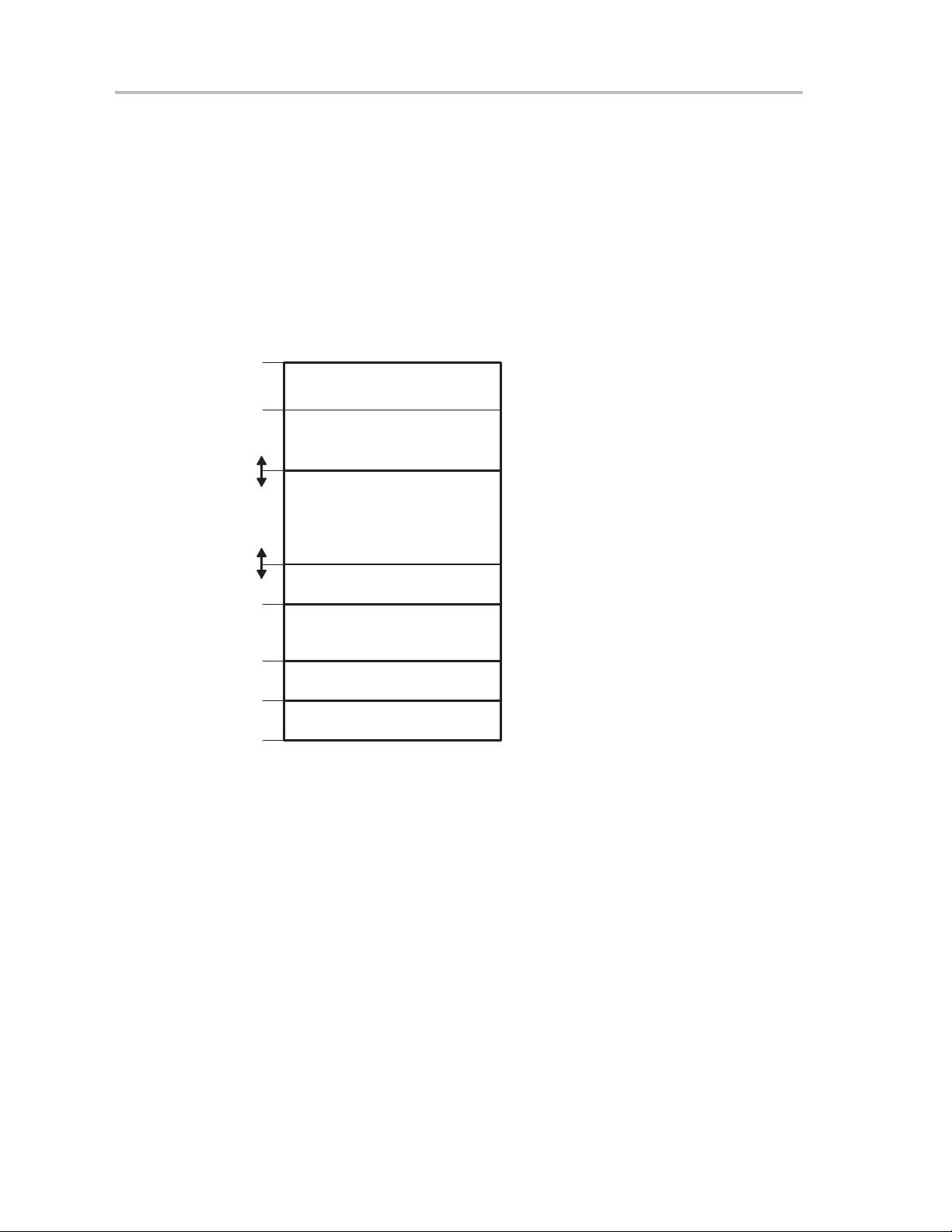
The MSP430 von-Neumann architecture has one address space shared with
special function registers (SFRs), peripherals, RAM, and Flash/ROM memory
as shown in Figure 1−2. See the device-specific data sheets for specific
memory maps. Code access are always performed on even addresses. Data
can be accessed as bytes or words.
The addressable memory space is 64 KB with future expansion planned.
Figure 1−2. Memory Map
0FFE0h
Interrupt Vector Table
Flash/ROM
RAM
16-Bit Peripheral Modules
8-Bit Peripheral Modules
Special Function Registers
0FFFFh
0FFDFh
0200h
01FFh
0100h
0FFh
010h
0Fh
0h
Access
Word/Byte
Word/Byte
Word
Byte
Byte
Word/Byte
1.4.1 Flash/ROM
The start address of Flash/ROM depends on the amount of Flash/ROM
present and varies by device. The end address for Flash/ROM is 0FFFFh.
Flash can be used for both code and data. Word or byte tables can be stored
and used in Flash/ROM without the need to copy the tables to RAM before
using them.
The interrupt vector table is mapped into the upper 16 words of Flash/ROM
address space, with the highest priority interrupt vector at the highest
Flash/ROM word address (0FFFEh).
1.4.2 RAM
RAM starts at 0200h. The end address of RAM depends on the amount of RAM
present and varies by device. RAM can be used for both code and data.
Address Space
1-5
Introduction
1.4.3 Peripheral Modules
Peripheral modules are mapped into the address space. The address space
from 0100 to 01FFh is reserved for 16-bit peripheral modules. These modules
should be accessed with word instructions. If byte instructions are used, only
even addresses are permissible, and the high byte of the result is always 0.
The address space from 010h to 0FFh is reserved for 8-bit peripheral modules.
These modules should be accessed with byte instructions. Read access of
byte modules using word instructions results in unpredictable data in the high
byte. If word data is written to a byte module only the low byte is written into
the peripheral register, ignoring the high byte.
1.4.4 Special Function Registers (SFRs)
Some peripheral functions are configured in the SFRs. The SFRs are located
in the lower 16 bytes of the address space, and are organized by byte. SFRs
must be accessed using byte instructions only. See the device-specific data
sheets for applicable SFR bits.
1.4.5 Memory Organization
Bytes are located at even or odd addresses. Words are only located at even
addresses as shown in Figure 1−3. When using word instructions, only even
addresses may be used. The low byte of a word is always an even address.
The high byte is at the next odd address. For example, if a data word is located
at address xxx4h, then the low byte of that data word is located at address
xxx4h, and the high byte of that word is located at address xxx5h.
Figure 1−3. Bits, Bytes, and Words in a Byte-Organized Memory
15
7
14
6
. . Bits . .
. . Bits . .
9
1
8
0
Byte
Byte
Word (High Byte)
Word (Low Byte)
xxxAh
xxx9h
xxx8h
xxx7h
xxx6h
xxx5h
xxx4h
xxx3h
2-1
System Resets, Interrupts, and Operating Modes
This chapter describes the MSP430x1xx system resets, interrupts, and
operating modes.
Topic Page
2.1 System Reset and Initialization 2-2. . . . . . . . . . . . . . . . . . . . . . . . . . . . . . . . .
2.2 Interrupts 2-6. . . . . . . . . . . . . . . . . . . . . . . . . . . . . . . . . . . . . . . . . . . . . . . . . . . .
2.3 Operating Modes 2-14. . . . . . . . . . . . . . . . . . . . . . . . . . . . . . . . . . . . . . . . . . . . .
2.4 Principles for Low-Power Applications 2-17. . . . . . . . . . . . . . . . . . . . . . . .
2.5 Connection of Unused Pins 2-17. . . . . . . . . . . . . . . . . . . . . . . . . . . . . . . . . . .
Chapter 2
System Reset and Initialization
2-2
System Resets, Interrupts, and Operating Modes
2.1 System Reset and Initialization
The system reset circuitry shown in Figure 2−1 sources both a power-on reset
(POR) and a power-up clear (PUC) signal. Different events trigger these reset
signals and different initial conditions exist depending on which signal was
generated.
Figure 2−1. Power-On Reset and Power-Up Clear Schematic
POR
Detect
V
CC
POR
Latch
S
S
R
PUC
Latch
S
S
R
Resetwd1
Resetwd2
S
S
Delay
RST/NMI
WDTNMI
†
WDTSSEL
†
WDTQn
†
WDTIFG
†
EQU
†
MCLK
POR
PUC
0 V
S
(from flash module)
KEYV
POR
Detect
#
V
CC
0 V
POR
Delay
#
V
CC
0 V
SVS_POR
§
0 V
V
CC
0 V
Brownout
Reset
‡
† From watchdog timer peripheral module
‡ Devices with BOR only
# Devices without BOR only
§ Devices with SVS only
~ 50us
A POR is a device reset. A POR is only generated by the following three
events:
- Powering up the device
- A low signal on the RST/NMI pin when configured in the reset mode
- An SVS low condition when PORON = 1.
A PUC is always generated when a POR is generated, but a POR is not
generated by a PUC. The following events trigger a PUC:
- A POR signal
- Watchdog timer expiration when in watchdog mode only
- Watchdog timer security key violation
- A Flash memory security key violation
System Reset and Initialization
2-3
System Resets, Interrupts, and Operating Modes
2.1.1 Power-On Reset (POR)
When the V
CC
rise time is slow, the POR detector holds the POR signal active
until V
CC
has risen above the V
POR
level, as shown in Figure 2−2. When the
V
CC
supply provides a fast rise time the POR delay, t
(POR_DELAY)
, provides
active time on the POR signal to allow the MSP430 to initialize.
On devices with no brownout-reset circuit, If power to the MSP430 is cycled,
the supply voltage V
CC
must fall below V
min
to ensure that a POR signal occurs
when V
CC
is powered up again. If V
CC
does not fall below V
min
during a cycle
or a glitch, a POR may not be generated and power-up conditions may not be
set correctly. In this case, a low level on RST
/NMI may not cause a POR and
a full power-cycle will be required. See device-specific datasheet for
parameters.
Figure 2−2. POR Timing
V
No POR
PORPOR
V
POR
V
t
(POR_DELAY)
t
(POR_DELAY)
Set Signal for
POR circuitry
min
V
CC(min)
V
CC
剩余413页未读,继续阅读
HBZGL166
- 粉丝: 0
- 资源: 1
上传资源 快速赚钱
- 我的内容管理 收起
- 我的资源 快来上传第一个资源
- 我的收益 登录查看自己的收益
- 我的积分 登录查看自己的积分
- 我的C币 登录后查看C币余额
- 我的收藏
- 我的下载
- 下载帮助
会员权益专享
最新资源
- 京瓷TASKalfa系列维修手册:安全与操作指南
- 小波变换在视频压缩中的应用
- Microsoft OfficeXP详解:WordXP、ExcelXP和PowerPointXP
- 雀巢在线媒介投放策划:门户网站与广告效果分析
- 用友NC-V56供应链功能升级详解(84页)
- 计算机病毒与防御策略探索
- 企业网NAT技术实践:2022年部署互联网出口策略
- 软件测试面试必备:概念、原则与常见问题解析
- 2022年Windows IIS服务器内外网配置详解与Serv-U FTP服务器安装
- 中国联通:企业级ICT转型与创新实践
- C#图形图像编程深入解析:GDI+与多媒体应用
- Xilinx AXI Interconnect v2.1用户指南
- DIY编程电缆全攻略:接口类型与自制指南
- 电脑维护与硬盘数据恢复指南
- 计算机网络技术专业剖析:人才培养与改革
- 量化多因子指数增强策略:微观视角的实证分析
资源上传下载、课程学习等过程中有任何疑问或建议,欢迎提出宝贵意见哦~我们会及时处理!
点击此处反馈
安全验证
文档复制为VIP权益,开通VIP直接复制
信息提交成功