
TI Information — Selective Disclosure
13
DRV3245E-Q1
www.ti.com
SLVSEE6 –APRIL 2019
Product Folder Links: DRV3245E-Q1
Submit Documentation FeedbackCopyright © 2019, Texas Instruments Incorporated
Electrical Characteristics (continued)
Over recommended operation conditions –40°C ≤ T
J
≤ +175°C, 4.5 V ≤ PVDD ≤ 45 V (unless otherwise noted)
ITEM NO. PARAMETER TEST CONDITIONS MIN TYP MAX UNIT
5.13.2 I
limit_AVDD
AVDD current limit PVDD = 14 V; AVDD is shorted to GND 25 100 mA
5.13.3 V
DVDD_UVLO
DVDD undervoltage fault Relative to GND 2.4 2.7 V
5.13.4 V
DVDD_OVLO
DVDD overvoltage fault Relative to GND 3.3 3.63 V
5.13.5
V
PVDD_UVFL
Undervoltage protection warning, PVDD
PVDD falling; 7.55 8.35
V
5.13.6 PVDD rising; 7.7 8.5
5.13.7
V
PVDD_UVLO
Undervoltage protection fault, PVDD
PVDD falling 4.1 4.5
V
5.13.8 PVDD rising 4.5 4.95
5.13.9
V
PVDD_OVFL
Overvoltage protection warning, PVDD
PVDD falling 32 35.5
V
5.13.10 PVDD rising 33 36.5
5.13.11 V
VCPH_UVLO
Charge-pump undervoltage protection
fault, VCPH
Relative to PVDD 4.42 4.95 V
5.13.12 V
VCP_LSD_UVLO
Low-side regulator undervoltage fault,
VCP_LSD
Relative to GND 6.4 7.5 V
5.13.13 l
limit_VCP_LSD
VCP_LSD current limit PVDD = 14 V; VCP_LSD is shorted to GND; 200 mA
5.13.14 V
VCP_LSD_OVLO
Low-side regulator overvoltage fault,
VSP_LSD
Relative to GND 13 15 V
5.13.15 V
VCPH_OVLO
Charge-pump overvoltage protection fault,
VCPH
Relative to PVDD 13 15 V
5.13.16 V
VCPH_OVLO_ABS
Charge-pump overvoltage protection fault,
VCPH
Relative to GND 52 57 V
5.13.17 t
degAVDD
AVDD OVLO/UVLO detection deglitch
time
8 10 μs
5.13.18 t
degDVDD
DVDD OVLO detection deglitch time 8 10 μs
5.13.19 t
degPVDD
PVDD OVFL/UVLO detection deglitch
time
8 10 μs
5.13.20 t
degVCPH
VCPH OVLO_ABS/OVLO/UVLO detection
deglitch time
8 10 μs
5.13.21 t
degVCP_LSD
VCP_LSD OVLO/UVLO detection deglitch
time
8 10 μs
5.13.22 E
clkmon
Clock Monitor error detection threshold –30% 30%
TEMPERATURE PROTECTION
5.14.0 OTW_CLR
Junction temperature to clear
overtemperature warning (OTW)
100 130 160 ℃
5.14.1 OTW_SET
Junction temperature for overtemperature
warning (OTW)
130 160 190 ℃
5.14.2 OTW2_CLR
Junction temperature to clear
overtemperature warning 2 (OTW2)
125 155 185 ℃
5.14.3 OTW2_SET
Junction temperature for overtemperature
warning 2 (OTW2)
155 185 215 ℃
5.14.4 t
degOTW
OTW detection deglitch time 8 10 µs
5.14.5 t
degOTW2
OTW2 detection deglitch time 2.5 6 12 µs
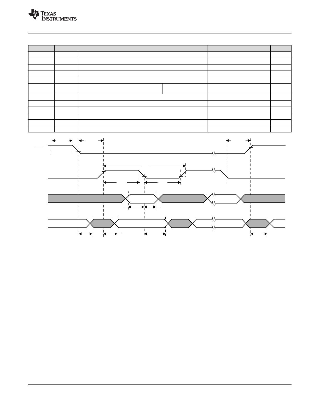
PROTECTION CONTROL
5.15.0 t
degDRVOFF
DRVOFF input deglitch time 1 2 4 µs
5.15.1 t
pd,DRVOFF_SD
Propagation delay of DRVOFF shutdown
After rising edge of DRVOFF to time until gate
drivers initiate shutdown
10 µs
5.15.2 t
degEN
EN input deglitch time 2 4 10 µs
5.15.3 t
pd,EN_SD
Propagation delay of EN shutdown
After falling edge of EN to time until gate drviers
initiate shutdown
25 µs
5.15.4 t
pd,ERR-L
Propagation delay from error event to
nFAULT reporting
After detecting error until nFAULT goes low;
deglitch time is not included.
5 µs
5.15.5 t
pd,ERR-SD
Propagation delay from error event to gate
driver shutdown
After detecting error until gate drivers initiate
shutdown
5 µs
FET CURRENT PROTECTION (VDS SENSING)
剩余73页未读,继续阅读


