HX8363-B单芯片TFT驱动器临时版本01,2010年10月
需积分: 9 48 浏览量
更新于2024-07-15
收藏 11.79MB PDF 举报
本文档是关于HX8363-B型号的TFT(Thin Film Transistor)移动单芯片驱动器的临时版本v01,发布日期为2010年10月11日,适用于TSE(可能是指特定客户或项目团队)。该驱动器具有480 x 864像素的分辨率,支持16.7百万色显示,内部集成GRAM(图形 RAM),旨在为小型显示屏提供高效且灵活的解决方案。
文档详细介绍了产品的特性、结构和接口,确保用户全面了解其功能和操作。以下是一些关键知识点:
1. **产品概述**:
- **尺寸与颜色**:480 RGB x 864 dot的屏幕尺寸,支持16.7 million color显示,能够提供丰富的色彩表现。
- **内建GRAM**:集成的GRAM技术有助于简化设计过程,减少外部存储需求。
2. **硬件规格**:
- **接口类型**:包括多种并行接口如24位、18位、16位、9位和8位,以及串行接口MIPIDBI-C,提供了不同的数据传输选项。
- **控制界面**:描述了设备与系统控制器之间的接口规范,便于编程和配置。
3. **物理设计**:
- **模块与布局**:文档提供了详细的模块描述和引脚分配,有助于硬件工程师进行电路板设计。
- **PAD坐标与凸点排列**:提供了关于连接器(PAD)的位置信息,包括凸点(bump)的布置,这对于PCB布局至关重要。
4. **安全与保密**:
- **版权声明**:文档声明所有信息为Himax的专有财产,未经许可不得复制或披露,体现了知识产权保护的重要性。
5. **文档分类**:
- **临时版本**:表明此文档尚在开发阶段,可能会在后续版本中更新和完善。
对于从事嵌入式系统设计、硬件工程师、或对TFT驱动器有兴趣的读者来说,这份文档是深入理解HX8363-B核心组件的重要参考资料,它涵盖了从基本规格到接口协议的全方位信息,对于实现高性能、高效率的显示解决方案具有实用价值。
-P.16-
HX8363-B
480RGBx864dots, TFT Mobile Single Chip Driver
DATA SHEET Temporary V01
Himax Confidential Temporary Version
This information contained herein is the exclusive property of Himax and shall not be distributed, reproduced, or disclosed
in whole or in part without prior written permission of Himax.
October, 2010
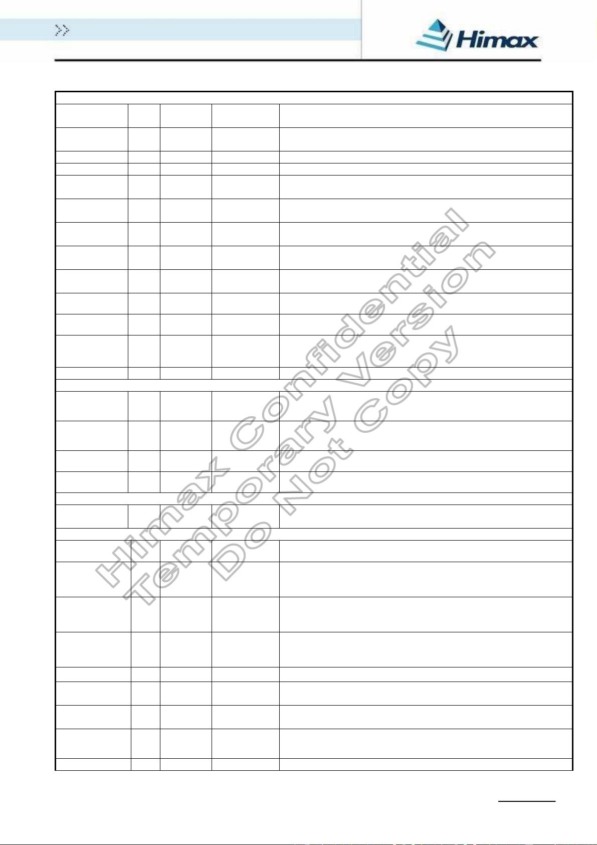
Output Pins of Power and reference voltage
VSP I 6
Stabilizing
capacitor
Input voltage from the set-up circuit (4.7V to 5.5V).
It is generated from
VDD3.
VSN I 6
Stabilizing
capacitor
Input voltage from the set-up circuit (-4.7V to -5.5V).
It is generated from
VDD3.
VSPC I 1 VSP
Positive boosting reference voltage input.
VSNC I 1 VSN
Negative boosting reference voltage input.
VSPR O 2
Stabilizing
capacitor
Positive regulated voltage output (3.5V ~ VSP - 0.5)
VSNR O 2
Stabilizing
capacitor
Negative regulated voltage output (-3.5V ~ VSN + 0.5)
VDDD O 6
Stabilizing
capacitor
Internal logic voltage output
VDDDN O 4
Stabilizing
capacitor
Internal logic voltage output (-2.5V fixed)
VREF O 2
Stabilizing
capacitor
Reference voltage from internal band gap circuit. The tolerance of VREF
voltage is ± 3 ﹪.(1.8V fixed)
VGH
O
5
Stabilizing
capacitor
Output voltage from the step-up circuit, it is generated from VSP and
VSN. Connect to a stabilizing capacitor between VSSA and VGH.
VGL
O
11
Stabilizing
capacitor
Output voltage from the step-up circuit, it is generated from VSP and
VSN. Connect to a stabilizing capacitor between VSSA and VGL.
VCOM O 17
Stabilizing
capacitor
The common voltage in DC com driving. The voltage range is set
between -2V to 0V. It must be connected a stabilizing capacitor 2.2u to
VSSD.
VCOMR I 1 -
This pin is used for external VCOM input.
DC/DC pumping
C21AP, C21AN
I/O 8
Step-up
Capacitor
Connect to the step-up capacitors according to the DC/DC
pumping factor by pumping the VGH voltage.
C22AP, C22AN
I/O 8
Step-up
Capacitor
Connect to the step-up capacitors according to the DC/DC
pumping factor by pumping the VGL voltage.
VCSW1 O 5 -
Boosting control output1, needs to connect to the CTRL_A of HX5186-A
or the gate pin of NMOS on external DC/DC converter circuit. (0~VDD3)
VCSW2 O 4 -
Boosting control output2, needs to connect to the CTRL_B of HX5186-A
or the gate pin of PMOS on external DC/DC converter circuit. (0~VDD3)
CABC & ABC & Ambient light sensor
CABC_PWM_
OUT
O 2 -
Backlight On/Off control pin. If use CABC function, the pin can connect
to external LED driver IC. The output voltage range = 0~ VDD1.
Test Pins
OSC I 1 -
Oscillator input for test purpose.
If not used, please let it open or connected to VSSD.(weak pull low)
TEST0 I 1 VSSD
A test pin. This pin is by internal logic function test.This pin can
output on FPC.
If not used, let it open or connected to VSSD.(weak pull low)
TEST1 I 1 VSSD
A test pin. This pin is by internal logic function test.This pin can
output on FPC. If not used, let it open or connected to
VSSD.(weak pull low)
TEST2 I 1 MPU
A test pin. This pin is by internal logic function test.This pin can
output on FPC. If not used, let it open or connected to
VSSD.(weak pull low)
TS7~0
O 8 Open
A test pin. Disconnect it.
VTESTOUTP
O 1 Open
A test pin. This pin can output on FPC for test use. Disconnect it
if no use.
VTESTOUTN
O 1 Open
A test pin. This pin can output on FPC for test use. Disconnect it
if no use.
DUMMYR1
DUMMYR2
- 2 Open
Dummy pads. Available for measuring the COG contact
resistance. They are short-circuited within the chip.
DUMMY - 50 Open Dummy pads. These pins are no function, please let them open.
For TSE Only
剩余269页未读,继续阅读
2023-07-13 上传
2023-07-16 上传
2023-04-25 上传
2023-07-16 上传
2023-06-13 上传
2023-06-06 上传
2023-03-28 上传

u010365054
- 粉丝: 5
- 资源: 1237
 我的内容管理
展开
我的内容管理
展开


最新资源
- AirKiss技术详解:无线传递信息与智能家居连接
- Hibernate主键生成策略详解
- 操作系统实验:位示图法管理磁盘空闲空间
- JSON详解:数据交换的主流格式
- Win7安装Ubuntu双系统详细指南
- FPGA内部结构与工作原理探索
- 信用评分模型解析:WOE、IV与ROC
- 使用LVS+Keepalived构建高可用负载均衡集群
- 微信小程序驱动餐饮与服装业创新转型:便捷管理与低成本优势
- 机器学习入门指南:从基础到进阶
- 解决Win7 IIS配置错误500.22与0x80070032
- SQL-DFS:优化HDFS小文件存储的解决方案
- Hadoop、Hbase、Spark环境部署与主机配置详解
- Kisso:加密会话Cookie实现的单点登录SSO
- OpenCV读取与拼接多幅图像教程
- QT实战:轻松生成与解析JSON数据
