Rev. A 02/16
5
INN21x3-21x5
www.power.com
The most likely event that could require an additional handshake is
when the primary stops switching resulting from a momentary line
drop-out or brown-out event. When the primary resumes operation,
it will default into a start-up condition and attempt to detect hand-
shake pulses from the secondary.
In the event the secondary does not detect that the primary responds
to requests for 6 consecutive cycles, or if the secondary detects that
the primary is switching without cycle requests for 6 or more
consecutive cycles, the secondary controller will initiate a second
handshake sequence.
This protection mode also provides additional protection against
cross-conduction of the SR MOSFET while the primary is switching.
This protection mode also prevents output overvoltage in the event
the primary is reset while the secondary is still in control and light/
medium load conditions exist.
Line Voltage Monitor
The VOLTAGE MONITOR pin is used for input under and overvoltage
sensing and protection function.
A 8 MW resistor is tied between the high voltage bulk DC capacitor
after the bridge or connected through a set of diodes from the AC
side of bridge and small high-voltage capacitor and bleed resistor
(for fast AC reset) and VOLTAGE MONITOR pin to enable this function.
To disable this function the VOLTAGE MONITOR pin should be tied to
the PRIMARY BYPASS pin.
At power-up after the BPP is charged and the I
LIM
is latched, prior to
switching the state of VOLTAGE MONITOR pin current is checked to
determine that it is above brown-in (I
UV+
) And below the overvoltage
shutdown threshold (I
OV+
) To proceed with start-up.
If during normal operation the VOLTAGE MONITOR pin current falls
below the brown-out (I
UV-
) threshold and remains below brown-in
(I
UV+
) for longer than t
UV-
the controller enters into auto-restart with
a short auto-restart off-time (~200 ms). Switching will only resume
once the VOLTAGE MONITOR pin current is above the brown-in
threshold (I
UV+
) for a time period exceeding ~150 ms.
In the event during normal operation the VOLTAGE MONITOR pin
current is above the overvoltage threshold (I
OV+
) for longer than t
OV
,
the controller will enter auto-restart with a short auto-restart off-time
(~200 ms). Switching will only resume once the VOLTAGE MONITOR
pin current fall below (I
OV-
)
for a time period exceeding ~150 ms.
Secondary Controller
Once the device enters the short auto-restart OFF-time, the PRIMARY
BYPASS pin will activate an internal bleed to discharge the input bulk
capacitor. The feedback driver block is the drive to the FluxLink
communication loop transferring switching pulse requests to the
primary IC.
As shown in the block diagram in Figure 4, the secondary controller
is powered through a 4.45 V Regulator block by either VOUT or
FORWARD pin connections to the SECONDARY BYPASS pin. The
SECONDARY BYPASS pin is connected to an external decoupling
capacitor and fed internally from the regulator block.
The FORWARD pin also connects to the negative edge detection
block used for both handshaking and timing to turn on the synchro-
nous rectier MOSFET (SR FET) connected to the SYNCHRONOUS
RECTIFIER DRIVE pin. The FORWARD pin is also used to sense when
to turn off the SR FET in discontinuous mode operation when the
voltage across the FET on resistance drops below V
SR(TH)
.
In continuous mode operation the SR FET is turned off when the
pulse request is sent to demand the next switching cycle, providing
excellent synchronization free of any overlap for the FET turn-off
while operating in continuous mode.
The mid-point of an external resistor divider network between the
VOUT and SECONDARY GROUND pins is tied to the FEEDBACK pin
to regulate the output voltage. The internal voltage comparator
reference voltage is V
REF
(1.265 V).
The external current sense resistor connected between IS and
SECONDARY GROUND pins is used to regulate the output current in
constant current regulator mode. The internal current sense
comparator threshold is IS
VTH
used to determine the value at which
the power supply output current is regulated.
Secondary Controller Oscillator
The typical oscillator frequency is internally set to an average
frequency of 100 kHz.
The oscillator incorporates circuitry that introduces a small amount of
frequency jitter, typically 6 kHz peak-to-peak, to minimize EMI
emission. The modulation rate of the frequency jitter is set to 1 kHz
to optimize EMI reduction for both average and quasi-peak emissions.
Output Overvoltage Protection
In the event the sensed voltage on the FEEDBACK pin is 2% higher
than the regulation threshold, a bleed current of ~10 mA is applied on
the VOUT pin. This bleed current increases to ~140 mA in the event
the FEEDBACK pin voltage is raised to beyond ~20% of the internal
FEEDBACK pin reference voltage. The current sink on the VOUT pin
is intended to discharge the output voltage for momentary overshoot
events. The secondary does not relinquish control to the primary
during this mode of operation.
FEEDBACK Pin Short Detection
In the event the FEEDBACK pin voltage is below the V
FB(OFF)
threshold
at start-up, the secondary will complete the primary/secondary hand-
shake and will stop requesting pulses to initiate an auto-restart. The
secondary will stop requesting cycles for t
AR(SK)
, to begin primary-side
auto-restart of t
AR(OFF)SH
. In this condition, the total apparent AR
off-time is t
AR(SK)
+ t
AR(OFF)SH
. During normal operation, the secondary
will stop requesting pulses from the primary to initiate an auto-restart
cycle when the FEEDBACK pin voltage falls below V
FB(OFF)
threshold.
The deglitch lter on the V
FB(OFF)
is less than 10 msec. The secondary
will relinquish control after detecting the FEEDBACK pin is shorted to
ground.
Cable Drop Compensation (CDC)
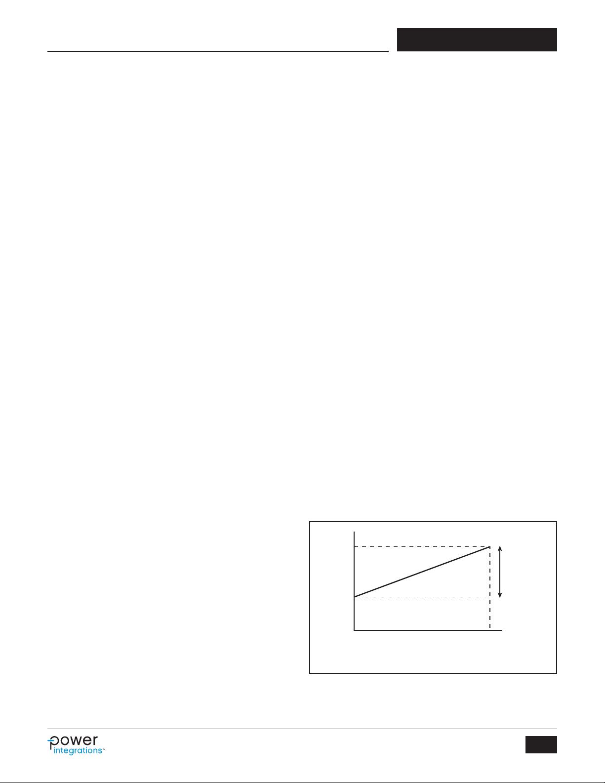
The amount of cable drop compensation is a function of the load with
respect to the constant current regulation threshold as illustrated in
Figure 7.
The lower feedback pin resistor must be tied to the SECONDARY
GROUND pin (not ISENSE pin) to have output cable drop compensa-
tion enabled.
PI-7863-010516
V
OUT
+
φ
CD
V
OUT
Onset of CC
Regulation
No-Load
Cable Drop
Compensation
Load Current
Output Voltage
End of PCB
Figure 7. Cable Drop Compensation Characteristics.


