
DS90C363B
SNLS179F –APRIL 2004–REVISED APRIL 2013
www.ti.com
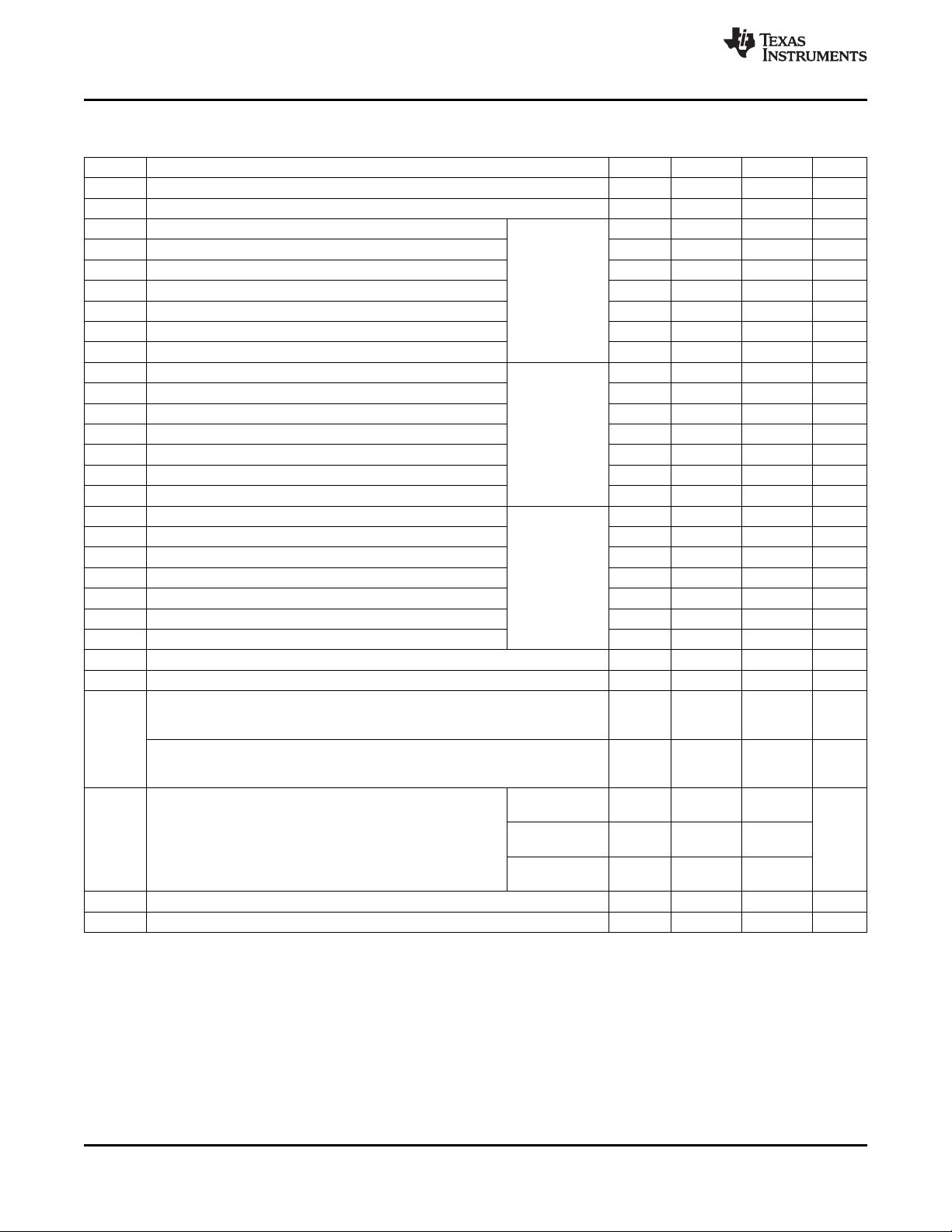
Transmitter Switching Characteristics
Over recommended operating supply and temperature ranges unless otherwise specified
Symbol Parameter Min Typ Max Unit
LLHT LVDS Low-to-High Transition Time (Figure 5 ) 0.75 1.4 ns
LHLT LVDS High-to-Low Transition Time (Figure 5 ) 0.75 1.4 ns
TPPos0 Transmitter Output Pulse Position for Bit 0 (Figure 12 )
(1)
−0.20 0 +0.20 ns
TPPos1 Transmitter Output Pulse Position for Bit 1 2.00 2.20 2.40 ns
TPPos2 Transmitter Output Pulse Position for Bit 2 4.20 4.40 4.60 ns
TPPos3 Transmitter Output Pulse Position for Bit 3 f = 65 MHz 6.39 6.59 6.79 ns
TPPos4 Transmitter Output Pulse Position for Bit 4 8.59 8.79 8.99 ns
TPPos5 Transmitter Output Pulse Position for Bit 5 10.79 10.99 11.19 ns
TPPos6 Transmitter Output Pulse Position for Bit 6 12.99 13.19 13.39 ns
TPPos0 Transmitter Output Pulse Position for Bit 0 (Figure 12 )
(1)
−0.25 0 +0.25 ns
TPPos1 Transmitter Output Pulse Position for Bit 1 3.32 3.57 3.82 ns
TPPos2 Transmitter Output Pulse Position for Bit 2 6.89 7.14 7.39 ns
TPPos3 Transmitter Output Pulse Position for Bit 3 f = 40 MHz 10.46 10.71 10.96 ns
TPPos4 Transmitter Output Pulse Position for Bit 4 14.04 14.29 14.54 ns
TPPos5 Transmitter Output Pulse Position for Bit 5 17.61 17.86 18.11 ns
TPPos6 Transmitter Output Pulse Position for Bit 6 21.18 21.43 21.68 ns
TPPos0 Transmitter Output Pulse Position for Bit 0 (Figure 12 )
(1)
−0.45 0 +0.45 ns
TPPos1 Transmitter Output Pulse Position for Bit 1 5.26 5.71 6.16 ns
TPPos2 Transmitter Output Pulse Position for Bit 2 10.98 11.43 11.88 ns
TPPos3 Transmitter Output Pulse Position for Bit 3 f = 25 MHz 16.69 17.14 17.59 ns
TPPos4 Transmitter Output Pulse Position for Bit 4 22.41 22.86 23.31 ns
TPPos5 Transmitter Output Pulse Position for Bit 5 28.12 28.57 29.02 ns
TPPos6 Transmitter Output Pulse Position for Bit 6 33.84 34.29 34.74 ns
TSTC TxIN Setup to TxCLK IN (Figure 7 ) 2.5 ns
THTC TxIN Hold to TxCLK IN (Figure 7 ) 0.5 ns
TCCD TxCLK IN to TxCLK OUT Delay (Figure 8 ) 50% duty cycle input clock is 3.340 7.211 ns
assumed, T
A
= −10°C, and 65MHz for "Min", T
A
= 70°C, and 25MHz for "Max",
V
CC
= 3.6V, R_FB = V
CC
TxCLK IN to TxCLK OUT Delay (Figure 8 ) 50% duty cycle input clock is 3.011 6.062 ns
assumed, T
A
= −10°C, and 65MHz for "Min", T
A
= 70°C, and 25MHz for "Max",
V
CC
= 3.6V, R_FB = GND
SSCG 100kHz ±
f = 25 MHz
2.5%/−5%
Spread Spectrum Clock support; Modulation frequency with a 100kHz ±
f = 40 MHz
linear profile
(2)
2.5%/−5%
100kHz ±
f = 65 MHz
2.5%/−5%
TPLLS Transmitter Phase Lock Loop Set (Figure 9 ) 10 ms
TPDD Transmitter Power Down Delay (Figure 11 ) 100 ns
(1) The Minimum and Maximum Limits are based on statistical analysis of the device performance over process, voltage, and temperature
ranges. This parameter is functionality tested only on Automatic Test Equipment (ATE).
(2) Care must be taken to ensure TSTC and THTC are met so input data are sampling correctly. This SSCG parameter only shows the
performance of tracking Spread Spectrum Clock applied to TxCLK IN pin, and reflects the result on TxCLKOUT+ and TxCLK− pins.
4 Submit Documentation Feedback Copyright © 2004–2013, Texas Instruments Incorporated
Product Folder Links: DS90C363B
剩余19页未读,继续阅读


