[AK4499]
019001308-E-00 2019/02
- 3 -
3. Table of Contents
1. General Description ........................................................................................................................ 1
2. Features .......................................................................................................................................... 1
3. Table of Contents ............................................................................................................................ 3
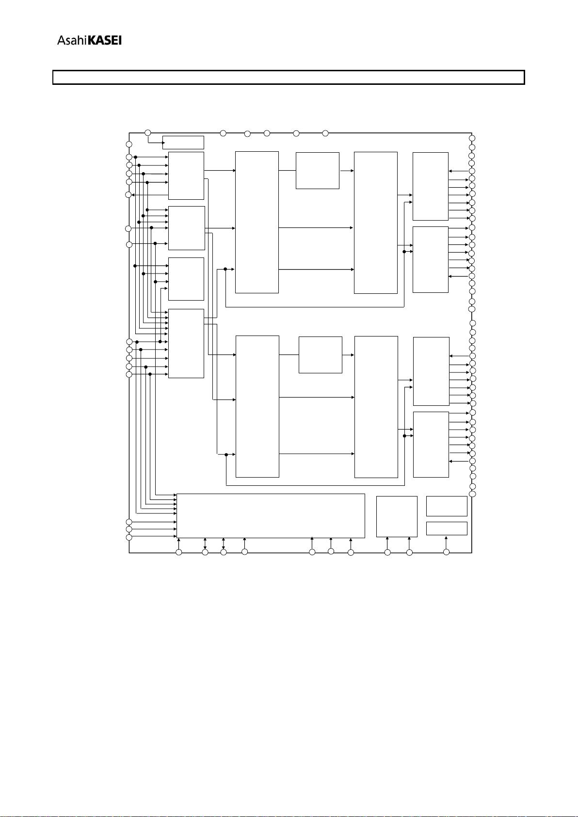
4. Block Diagram and Functions ......................................................................................................... 4
4.1. Block Diagram ................................................................................................................................. 4
4.2. Functions ......................................................................................................................................... 5
5. Pin Configurations and Functions ................................................................................................... 6
5.1. Pin Configurations ........................................................................................................................... 6
5.2. Functions ......................................................................................................................................... 7
5.3. Handling of Unused Pin .................................................................................................................. 11
6. Absolute Maximum Ratings .......................................................................................................... 13
7. Recommended Operating Conditions .......................................................................................... 14
8. Electical Characteristics ................................................................................................................ 15
8.1. Analog Characteristics ................................................................................................................... 15
8.2. DAC Digital Filter Characteristics (PCM Mode) ............................................................................ 19
8.3. DAC Digital-Filter Characteristics (DSD Mode) ............................................................................. 29
8.4. DC Characteristics ......................................................................................................................... 30
8.5. Switching Characteristics .............................................................................................................. 31
8.6. Timing Diagram .............................................................................................................................. 36
9. Functional Descriptions ................................................................................................................ 41
9.1. Control Mode ................................................................................................................................. 41
9.2. D/A Conversion Mode .................................................................................................................... 42
9.3. System Clock ................................................................................................................................. 45
9.4. Audio Interface Format .................................................................................................................. 51
9.5. Digital Filter .................................................................................................................................... 64
9.6. De-emphasis Filter (PCM Mode) ................................................................................................... 65
9.7. Digital Attenuator ........................................................................................................................... 66
9.8. Gain Adjustment Function ............................................................................................................. 67
9.9. Zero Detection, DSD Full-scale Detection .................................................................................... 68
9.10. LR Channel Output Signal Select, Phase Inversion Function .................................................... 73
9.11. PCM/DSD, EXDF/DSD Automatic Mode Switching Function ..................................................... 74
9.12. LDO .............................................................................................................................................. 83
9.13. Power Up/Down Sequence ......................................................................................................... 84
9.14. Power Down, Standby and Reset Function ................................................................................ 89
9.15. Synchronize Function (PCM Mode, EXDF Mode) ...................................................................... 93
9.16. Register Control Interface............................................................................................................ 95
9.17. Register Map ............................................................................................................................... 99
9.18. Register Definitions ................................................................................................................... 100
10. Recommended External Circuits ................................................................................................ 106
10.1. External Connection Example ................................................................................................... 106
10.2. Grounding and Power Supply Decoupling ................................................................................ 108
10.3. Reference Voltage ..................................................................................................................... 108
10.4. Analog Output ............................................................................................................................ 108
11. Package .......................................................................................................................................114
11.1. Outline Dimensions (HTQFP14 x 14-128, Unit: mm) ...........................................................114
11.2. Material & Terminal Finish .....................................................................................................115
11.3. Marking ..................................................................................................................................115
12. Ordering Guide ............................................................................................................................116
13. Revision Histroy ...........................................................................................................................116
IMPORTANT NOTICE ...........................................................................................................................117


 我的内容管理
收起
我的内容管理
收起
 我的收益 登录查看自己的收益
 我的积分
登录查看自己的积分
我的积分
登录查看自己的积分
 我的C币
登录后查看C币余额
我的C币
登录后查看C币余额
 我的收藏
我的收藏  我的下载
我的下载  下载帮助
下载帮助 


评论0